Low-Temperature (≤400°C) Deposition of High-Quality Dielectric and Passivation Films Using a 1200°C Dual-Zone PECVD System

Table of Contents

Introduction

As device architectures continue to scale down and diversify, the demand for low-temperature deposition of high-quality dielectric and passivation films has become increasingly critical. Advanced applications such as flexible electronics, heterojunction solar cells, MEMS devices, and back-end semiconductor processing often impose strict thermal budgets, typically ≤400°C.

Conventional thermal CVD processes struggle to meet these requirements without sacrificing film density, uniformity, or electrical performance. In this context, the 1200°C dual-zone PECVD (Plasma-Enhanced Chemical Vapor Deposition) system provides a powerful and flexible solution, enabling excellent film quality at low substrate temperatures through precise thermal and plasma control.

This article explores the process principles, film characteristics, and practical advantages of using a high-temperature dual-zone PECVD system for low-temperature dielectric and passivation film deposition.

Fundamentals of PECVD Technology

PECVD relies on plasma to dissociate precursor gases into highly reactive radicals, allowing thin-film growth at significantly reduced substrate temperatures compared to thermal CVD. Typical dielectric materials deposited by PECVD include:

  • Silicon nitride (SiNx)

  • Silicon oxide (SiOx)

  • Silicon oxynitride (SiON)

  • Hydrogenated amorphous silicon (a-Si:H)

Why High-Temperature Capability Matters for Low-Temperature Deposition

Although the substrate temperature remains low, the 1200°C-rated heating zone plays a crucial role in film quality:

  • Efficient precursor decomposition: High temperatures ensure stable and complete dissociation of gases such as SiH₄, NH₃, N₂O, and O₂.

  • Improved plasma uniformity: Stable plasma chemistry reduces particle formation and compositional fluctuations.

  • Reduced hydrogen-related defects: Enhanced gas-phase reactions help minimize excessive hydrogen incorporation in the film.

As a result, films deposited at ≤400°C exhibit properties comparable to those produced at much higher substrate temperatures in conventional systems.

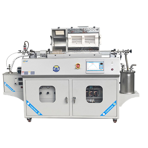
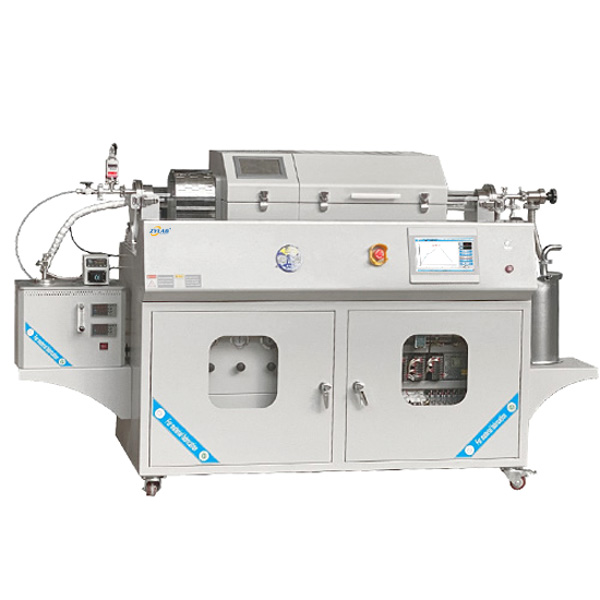
Film Quality Characteristics at ≤400°C

1. High Film Density and Low Defect Density

Dual-zone PECVD enables the formation of dense dielectric films with:

  • Low pinhole density

  • Reduced microvoids

  • Improved barrier properties

This is especially important for gate dielectrics and surface passivation layers where leakage current and reliability are critical.

2. Excellent Thickness Uniformity and Conformality

Optimized plasma distribution and gas flow design result in:

  • Thickness uniformity typically within ±2–3%

  • Good step coverage on structured or textured surfaces

  • Consistent refractive index across large substrates

These features are essential for semiconductor wafers and photovoltaic cells.

3. Tunable Film Stress

Film stress can be precisely adjusted by controlling:

  • Plasma power

  • Gas ratios (e.g., SiH₄/NH₃)

  • Substrate temperature

This enables low-stress or stress-balanced films, reducing the risk of cracking, delamination, or wafer bowing.

4. Superior Electrical and Passivation Performance

Low-temperature PECVD films deposited using a dual-zone system demonstrate:

  • High dielectric strength

  • Low leakage current

  • Excellent surface and bulk passivation

For example, SiNx films can achieve low surface recombination velocities, making them ideal for high-efficiency solar cells and advanced CMOS devices.

Application Areas

Semiconductor Manufacturing

  • Gate dielectrics and interlayer dielectrics

  • Passivation layers for CMOS and power devices

  • Back-end-of-line (BEOL) processing

Photovoltaics

  • SiNx passivation and anti-reflection coatings

  • Heterojunction and PERC solar cells

  • Thin-film photovoltaic technologies

Flexible and Organic Electronics

  • OLED encapsulation layers

  • Thin-film transistor (TFT) dielectrics

  • Wearable and bendable electronics

MEMS and Sensors

  • Electrical insulation layers

  • Environmental and chemical protection coatings

  • Stress-engineered functional films

Advantages for Research and Process Development

For R&D laboratories and pilot lines, a 1200°C dual-zone PECVD system offers:

  • Wide process window: Suitable for multiple materials and applications

  • High reproducibility: Stable plasma and temperature control

  • Scalability: Easy transition from research to small-scale production

  • Customization: Flexible configuration for different substrate sizes and gases

Conclusion

The 1200°C dual-zone PECVD system represents an advanced platform for low-temperature (≤400°C) deposition of high-quality dielectric and passivation films. By decoupling precursor activation from substrate heating, it delivers dense, uniform, low-defect films while preserving compatibility with temperature-sensitive substrates.

For researchers and engineers working in semiconductors, photovoltaics, MEMS, and flexible electronics, this technology provides an optimal balance between film performance, process flexibility, and thermal safety—making it an indispensable tool for next-generation device development.

Get In Touch

Fill out the form below — free quote and professional suggestion will be sent for reference very soon!